- 您现在的位置:买卖IC网 > Sheet目录316 > BU9847GUL-WE2 (Rohm Semiconductor)IC EEPROM 4KBIT 2WIRE VCSP50L1
BU9847GUL-W (4Kbit)
Datasheet
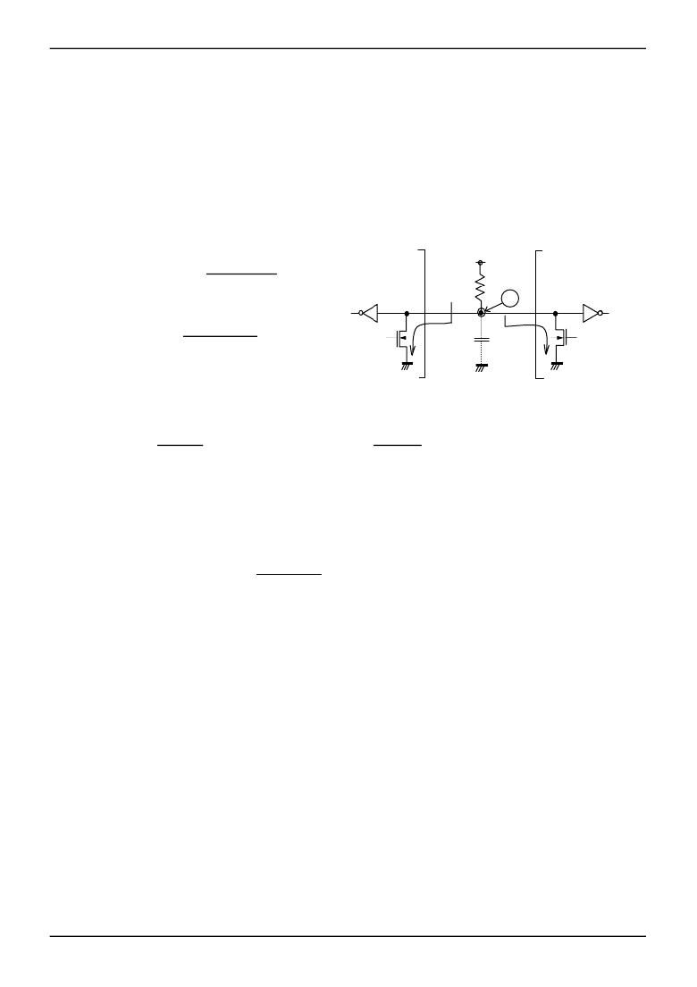
● I/O peripheral circuit
○ Pull up resistance of SDA terminal
SDA is NMOS open drain, so requires pull up resistance. As for this resistance value (R PU ), select an appropriate value to
this resistance value from microcontroller V IL , I L , and V OL -I OL characteristics of this IC. If R PU is large, action frequency is
limited. The smaller the R PU , the larger the consumption current at action.
○ Maximum value of R PU
The maximum value of R PU is determined by the following factors.
(1) SDA rise time to be determined by the capacity (CBUS) of bus line of R PU and SDA should be tR or below.
And AC timing should be satisfied even when SDA rise time is late.
(2) The bus electric potential A to be determined by input leak total (I L ) of device connected to bus at output of “H” to
SDA bus and R PU should sufficiently secure the input “H” level (V IH ) of microcontroller and EEPROM including
recommended noise margin 0.2Vcc.
V CC -I L R PU -0.2 V CC ≧ V IH
Microcontroller
BU9847GUL-W
∴
R PU ≦
0.8V CC -V IH
I L
R PU
Ex.) When V CC =3V, I L =10 μ A, V IH =0.7 Vcc
from (2)
A
SDA terminal
10×10
R PU ≦
0.8×3-0.7×3
-6
IL
Bus line
IL
≦
○ Minimum value of R PU
300 [ k ? ]
capacity CBUS
Figure 44. I/O circuit diagram
The minimum value of R PU is determined by the following factors.
(1) When IC outputs LOW, it should be satisfied that V OLMAX = 0.4V and I OLMAX = 3mA.
V CC -V OL
R PU
≦ I OL
∴ R PU ≧
V CC -V OL
I OL
(2) V OLMAX = 0.4V should secure the input “L” level (VIL) of microcontroller and EEPROM including recommended noise
margin 0.1V CC .
V OLMAX ≦ V IL – 0.1V CC
Ex.) When V CC = 3V, V OL = 0.4V, I OL = 3mA, microcontroller, EEPROM V IL = 0.3V CC
3 x 10
From (1),
∴ R PU ≧
3-0.4
-3
≧ 867[ ? ]
And
V OL = 0.4[V]
V IL = 0.3 x 3
=0.9 [V]
Therefore, the condition (2) is satisfied.
○ Pull up resistance of SCL terminal
When SCL control is made at CMOS output port, there is no need, but in the case there is timing where SCL becomes
“Hi-Z”, add a pull up resistance. As for the pull up resistance, one of several k ? to several ten k ? is recommended in
consideration of drive performance of output port of microcontroller.
● A2, WP process
○ Process of device address terminals (A2)
Check whether the set device address coincides with device address input sent from the master side or not, and select
one among plural devices connected to a same bus. Connect this terminal to pull up of pull down, or V CC or GND.
○ Process of WP terminal
WP terminal is the terminal that prohibits and permits write in hardware manner. In “H” status, only READ is available and
WRITE of all addresses is prohibited. In the case of “L”, both are available. In the case to use it as an ROM, it is
recommended to connect it to pull up or V CC . In the case to use both READ and WRITE, control WP terminal or connect it
to pull down or GND.
www.rohm.com
? 2012 ROHM Co., Ltd. All rights reserved.
TSZ22111 ? 15 ? 001
18/24
TSZ02201-0R2R0G100480-1-2
4.SEP.2012 Rev.001
发布紧急采购,3分钟左右您将得到回复。
相关PDF资料
BU9880GUL-WE2
IC EEPROM 64KBIT 2WIRE VCSP50L1
BU9882FV-WE2
IC EEPROM 2KBIT 400KHZ 14SSOP
BU9883FV-WE2
IC EEPROM 6KBIT 400KHZ SSOP16
BU9889GUL-WE2
IC EEPROM 8KBIT 2WIRE VCSP50L1
BU9891GUL-WE2
IC EEPROM 4KBIT VCSP T/R
BU9897GUL-WE2
IC EEPROM SERIAL VCSP50L2
BU99901GUZ-WE2
IC EEPROM 32KBIT 2WIRE VCSP
BUK218-50DY,118
TOPFET DUAL SWITCH D2PAK
相关代理商/技术参数
BU98570CH-3BW
制造商:ROHM 制造商全称:Rohm 功能描述:65,536 Colors 98RGB x 70 STN LCD control driver
BU98582CH-3BW
制造商:ROHM 制造商全称:Rohm 功能描述:65,536 Colors 104RGB x 82 STN LCD control driver
BU98664CH-3BW
制造商:ROHM 制造商全称:Rohm 功能描述:65,536 Colors 132RGB x 164 STN LCD control driver
BU9873F-GTE2
功能描述:Real Time Clock (RTC) IC Clock/Calendar I2C, 2-Wire Serial 8-SOIC (0.173", 4.40mm Width) 制造商:rohm semiconductor 系列:- 包装:剪切带(CT) 零件状态:有效 类型:时钟/日历 特性:警报器,闰年 存储容量:- 时间格式:HH:MM:SS(12/24 小时) 日期格式:YY-MM-DD-dd 接口:I2C,2 线串口 电压 - 电源:1.8 V ~ 5.5 V 电压 - 电源,电池:- 电流 - 计时(最大):1μA ~ 1.35μA @ 3V ~ 5.5V 工作温度:-40°C ~ 85°C 安装类型:表面贴装 封装/外壳:8-SOIC(0.173",4.40mm 宽) 供应商器件封装:8-SOP 标准包装:1
BU9873FJ-GTE2
功能描述:Real Time Clock (RTC) IC Clock/Calendar I2C, 2-Wire Serial 8-SOIC (0.154", 3.90mm Width) 制造商:rohm semiconductor 系列:- 包装:剪切带(CT) 零件状态:有效 类型:时钟/日历 特性:警报器,闰年 存储容量:- 时间格式:HH:MM:SS(12/24 小时) 日期格式:YY-MM-DD-dd 接口:I2C,2 线串口 电压 - 电源:1.8 V ~ 5.5 V 电压 - 电源,电池:- 电流 - 计时(最大):1μA ~ 1.35μA @ 3V ~ 5.5V 工作温度:-40°C ~ 85°C 安装类型:表面贴装 封装/外壳:8-SOIC(0.154",3.90mm 宽) 供应商器件封装:* 标准包装:1
BU9873FVM-GTTR
功能描述:Real Time Clock (RTC) IC Clock/Calendar I2C, 2-Wire Serial 8-VSSOP, 8-MSOP (0.110", 2.80mm Width) 制造商:rohm semiconductor 系列:- 包装:剪切带(CT) 零件状态:有效 类型:时钟/日历 特性:警报器,闰年 存储容量:- 时间格式:HH:MM:SS(12/24 小时) 日期格式:YY-MM-DD-dd 接口:I2C,2 线串口 电压 - 电源:1.8 V ~ 5.5 V 电压 - 电源,电池:- 电流 - 计时(最大):1μA ~ 1.35μA @ 3V ~ 5.5V 工作温度:-40°C ~ 85°C 安装类型:表面贴装 封装/外壳:8-VSSOP,8-MSOP(0.110",2.80mm 宽) 供应商器件封装:8-MSOP 标准包装:1
BU9873FVT-GE2
功能描述:Real Time Clock (RTC) IC Clock/Calendar I2C, 2-Wire Serial 8-TSSOP (0.173", 4.40mm Width) 制造商:rohm semiconductor 系列:- 包装:剪切带(CT) 零件状态:有效 类型:时钟/日历 特性:警报器,闰年 存储容量:- 时间格式:HH:MM:SS(12/24 小时) 日期格式:YY-MM-DD-dd 接口:I2C,2 线串口 电压 - 电源:1.8 V ~ 5.5 V 电压 - 电源,电池:- 电流 - 计时(最大):1μA ~ 1.35μA @ 3V ~ 5.5V 工作温度:-40°C ~ 85°C 安装类型:表面贴装 封装/外壳:8-TSSOP(0.173",4.40mm 宽) 供应商器件封装:8-TSSOP-B 标准包装:1
BU9873NUX-TTR
功能描述:Real Time Clock (RTC) IC Clock/Calendar I2C, 2-Wire Serial 8-UFDFN Exposed Pad 制造商:rohm semiconductor 系列:- 包装:剪切带(CT) 零件状态:有效 类型:时钟/日历 特性:警报器,闰年 存储容量:- 时间格式:HH:MM:SS(12/24 小时) 日期格式:YY-MM-DD-dd 接口:I2C,2 线串口 电压 - 电源:1.8 V ~ 5.5 V 电压 - 电源,电池:- 电流 - 计时(最大):1μA ~ 1.35μA @ 3V ~ 5.5V 工作温度:-40°C ~ 85°C 安装类型:表面贴装 封装/外壳:8-UFDFN 裸露焊盘 供应商器件封装:VSON008X2030 标准包装:1
